HD-FDD: Enabling Cost-Effective, Power-Efficient IoT Device Design

By Guy Cohen, Director Product Management

Cellular IoT is everywhere — monitoring city infrastructure, tracking assets, measuring agricultural data, and reading smart meters. Scaling IoT brings critical challenges: devices need to be both affordable and reliable. They must run for years on a single battery, meet carrier-grade standards, and work flawlessly everywhere — from city centers to remote locations, where maintenance isn’t an option. When a single device failure can eliminate ROI, there’s no room for compromise.

Sony Semiconductor Israel has pioneered cellular IoT technology, leveraging proven approaches like HD-FDD — a fundamental technology in LTE-M and NB-IoT with proven benefits that make it essential for future IoT standards. With over a decade of experience, SSI knows how to help device vendors build competitive products that meet real-world demands.

The Evolution of IoT Device Requirements

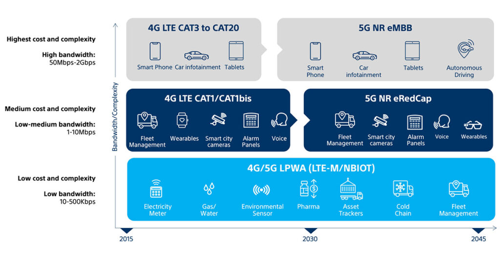
Today’s cellular IoT landscape divides into two main categories: LTE-M and NB-IoT serve low-power wide-area (LPWA) applications, while emerging 5G standards like eRedCap address mid-range IoT use cases. Traditional cellular devices prioritize high throughput and network capacity, but IoT applications require:

  • Cost efficiency for large-scale deployments
  • Extended battery life for remote operations
  • Global scalability across different regions and networks
  • Reliable coverage, including in challenging environments

These requirements drive innovation in device design, particularly in RF front-end architecture.

HD-FDD: A Simplified Approach to RF Design

FDD systems work like a two-lane highway — one lane for incoming traffic, one for outgoing, running simultaneously. This operation mode requires complex design on the device side, including duplex filters to manage RF signals. HD-FDD still uses separate frequencies for downlink and uplink like FDD, but doesn’t transmit and receive at the same time. 

This simpler device design eliminates the need for duplex filters, which maintains signal quality while reducing costs and complexity, making it more cost-effective and efficient for many applications.

HD-FDD vs FDD

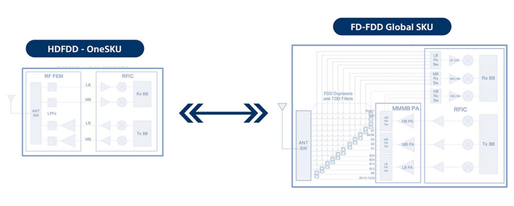
With this simplified RF architecture, HD-FDD delivers four key advantages:

  • Reduced bill of materials (BOM) cost through eliminated components
  • Improved power consumption and reduced peak current 
  • Enhanced flexibility for global deployment across regions
  • Simplified PCB design for more efficient manufacturing

Quantifiable Benefits for Device Vendors

For IoT device manufacturers competing in tight-margin markets, HD-FDD’s technical advantages translate directly to business results. The simplified design reduces development risks, accelerates time to market, and enables profitable scaling — especially critical when rapid deployment can make or break market success.

HD-FDD delivers four core business advantages:

  1. Lower Production Costs
    • Significant cost savings per unit by eliminating SAW/BAW duplexers
    • Reduced manufacturing complexity through simpler PCB design
    • Lower inventory costs with single SKU design

  2. Reduced Time to Market
    • Faster development cycles with simplified RF design
    • Single global certification process instead of regional variants
    • Reduced validation time through proven technology

  3. Performance at Scale
    • Extended battery life through superior power efficiency
    • Improved coverage with enhanced receiver sensitivity
    • Simplified thermal management with lower peak power consumption

  4. Global Scalability & Future-Readiness
    • One design for worldwide markets
    • Ready for emerging 5G IoT standards
    • Proven in millions of devices globally
    • Full support from SSI’s development tools and expertise

Quantifiable Benefits for Device Vendors

Implementation Considerations

While HD-FDD delivers significant advantages, successful implementation requires careful attention to three key design challenges: 

  • RF design quality. Today’s IoT chips pack multiple functions — baseband, RF, MCU, and location capabilities — onto a single chip. Traditional designs use SAW filters to clean up RF signals, but HD-FDD’s filter-free approach requires a different strategy.

    Think of it like a professional recording studio versus a podcast setup: without specialized filtering equipment, you need excellent baseline sound quality. Similarly, HD-FDD demands fundamentally clean RF design from the start.

    SSI addresses these design challenges through both hardware and software innovations, ensuring clean signal quality without relying on expensive filtering components.

  • Timing and Switching. HD-FDD’s approach of alternating between sending and receiving creates a unique challenge: The system needs to smoothly switch between different frequencies while maintaining precise timing. This requires accurate control of the RF systems, particularly during the crucial moments of switching between transmission and reception.
  • Performance Integration. Making these elements work together efficiently is key to unlocking HD-FDD’s benefits. While the technical implementation is complex, the result is straightforward: Device vendors get the cost and power advantages of HD-FDD while maintaining the reliable performance their products demand.

Getting RF design right creates lasting competitive advantage through both cost structure and performance — setting products apart from designs that rely on expensive components.

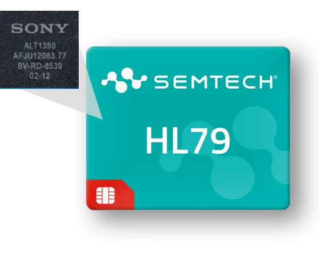
Recent advances in semiconductor technology, such as Sony’s ALT1350 cellular IoT chipset, demonstrate how these challenges can be effectively addressed while maximizing the benefits of HD-FDD architecture: Reduced BOM costs through eliminating SAW/BAW filters, enhanced power efficiency for longer battery life, and proven RF performance that meets carrier certification requirements worldwide. 

For vendors, this means faster time to market with globally deployable products that maintain high performance while reducing production costs.

Looking Ahead: HD-FDD in 5G IoT

5G IoT is coming, and HD-FDD technology is already part of the 5G ecosystem through LTE-M and NB-IoT, proving its value for IoT applications. Given HD-FDD’s success in these deployments, SSI believes strongly that it should be adopted in 5G Release 18 eRedCap for next-generation IoT products.

The math is simple: When you’re scaling from thousands to millions of IoT devices, small cost savings create major competitive advantages. HD-FDD’s specific technical features for 5G — including 5MHz bandwidth support and relaxed coexistence conditions — help vendors hit the market’s demanding targets:

  • Lower per-unit production costs
  • Extended battery life
  • Reliable performance at scale
  • Global deployment capability

Partnering with SSI means accessing both cutting-edge technology and proven IoT expertise. As enterprises roll out large-scale IoT deployments, they need solutions that balance strict budgets with carrier-grade performance. HD-FDD technology delivers exactly what it takes to win and execute these contracts.

Dual Mode (Satellite/Terrestrial) IoT terminals have the potential to revolutionize the IoT industry

Sony has recently enabled its flagship IoT chipset, ALT1250, with terrestrial network (TN) L-band support, expanding its already powerful capabilities to further enhance the operation of commercial IoT devices and networks.

Sony’s ALT1250 chipset, already available for commercial devices, supports satellite (NTN) L-Band operation, standardized in 3GPP as band 255.

The addition of L-band terrestrial band support, i.e., 3GPP Band 24, enables commercial IoT devices to operate on the L-band in both TN and NTN (non-terrestrial network) modes, with the potential to significantly improve availability and efficiency through a more seamless transition of devices between satellite and terrestrial network components.

IoT terminals can be connected to terrestrial networks when within terrestrial coverage areas and switch smoothly to satellite operation within the same L-band spectrum when outside of terrestrial coverage. This dual-mode capability opens up a world of possibilities for IoT applications across various industries.

Use Cases for dual mode TN/NTN operation for IoT

The integration of Non-Terrestrial Networks (NTN) with IoT devices enables a wide range of applications that were previously challenging or impossible to implement. Some key use cases include:

Asset Tracking: Global tracking of high-value assets, shipping containers, and vehicles across remote areas.

Agriculture: Monitoring crop health, soil conditions, and livestock in rural and remote farmlands.

Environmental Monitoring: Collecting data from sensors in forests, oceans, and other hard-to-reach locations for climate research and natural disaster prediction.

Maritime and Aviation: Ensuring continuous connectivity for ships and aircraft, enabling real-time monitoring and communication.

Emergency Services: Providing reliable communication in disaster-stricken areas where terrestrial networks may be compromised.

Utility Networks: Mostly relying on terrestrial coverage with public and private networks, device will be able to communicate thorough satellites in case of poor coverage or network outage.

The Power of NTN for IoT

NTN technology offers several advantages for IoT applications:

Coverage: Extending far beyond the reach of terrestrial networks, satellite NTN networks provide ubiquitous and always-on connectivity over a much wider area than traditional wireless network.

Reliability: NTN provides an additional layer of network reliability, ensuring critical endpoints maintain service continuity and operate seamlessly across networks.

Cost-Effectiveness: Using 3GPP standards-based technology, mobile satellite service providers can leverage mobile terrestrial volumes, making use of mainstream, low-cost IoT chipsets and devices which support both satellite and terrestrial connectivity. This approach minimizes the cost differential between terrestrial-only and hybrid terrestrial/satellite devices.

Efficient Resource Utilization: The dual-mode capability allows for the most efficient use of resources, seamlessly switching between terrestrial and satellite networks as needed.

Outlook for L-Band Technology

In the US, L-band is unique in that it is licensed and standardized for both satellite and terrestrial use. While terrestrial L-band networks are currently not deployed in the United States, Sony’s enhanced band support ensures that the device ecosystem is ready today and can be activated when networks are ready.

Using 3GPP standards-based technology, mobile satellite service providers can leverage mobile terrestrial volumes, making use of mainstream, low-cost IoT chipsets and devices which support both satellite and terrestrial connectivity. This approach minimizes the cost differential between terrestrial-only and hybrid terrestrial/satellite devices.

Extending far beyond the reach of terrestrial networks, the satellite NTN networks provide ubiquitous and always-on connectivity over a much wider area than traditional wireless networks. 3GPP standards-based devices allow critical endpoints to maintain service continuity, operate seamlessly across networks, and enable the most efficient use of resources while providing an additional layer of network reliability.

Leading the Future of Low-Power IoT: A Conversation with Semtech and Sony Altair on the New HL7900 Module

As the world continues to embrace the Internet of Things (IoT), the demand for low-power, high-efficiency solutions grows exponentially. At the forefront of this technological evolution stand two industry experts: Sony Altair and Semtech. Their latest innovation, the Semtech HL7900 module—a global 5G LPWA module featuring the Sony ALT1350 chipset—promises to revolutionize the IoT landscape by providing ultra-low power, future-ready connectivity.

Sony Altair Semtech

In this blog, we discuss with key leaders from Semtech and Sony Altair to explore how this cutting-edge module is poised to shape the future of IoT, unlocking new possibilities for smart cities, metering, asset tracking, and beyond.

Guy Cohen Sony
Michael Buonassisi Semtech

Hi Guy and Michael, let’s start with the vision behind the development of the new HL7900/ALT1350. What are the most critical needs and challenges faced by organizations when developing a successful cellular IoT device?

Michael: One major challenge is achieving low power consumption and extended battery life, which are essential for devices expected to last up to 20 years in the field. Customers often find it challenging to design a product that maintains low power consumption and long battery life across varying environments and network conditions. Another critical aspect is the complexity of deployments.  Wireless IoT is complex, and seamless integration isn’t always straightforward. Improving customer experience through clear documentation, intuitive software, user-friendly APIs, and robust development boards is crucial.

Guy: IoT use cases also increasingly demand higher levels of integration—combining multiple functionalities into single hardware or chipset solutions. This approach simplifies the overall solution and reduces the cost of end-to-end implementation. However, keeping APIs and interfaces simple and straightforward is equally important. Clear and concise documentation is essential to ensure ease of use when developing and deploying these devices in real-world applications.

How do the new Sony ALT1350 chipset and Semtech HL7900 module help solve these challenges?

Guy: From a chipset perspective, the ALT1350 significantly outperforms previous generations. Battery-operated devices can now achieve up to 4 times longer battery life for typical use cases. Additionally, the ALT1350 offers a high level of integration to meet the simplification need we’ve talked about earlier. It integrates more functions, such as location capabilities and additional short-range radio, which enhance connectivity and enable more use cases. It can, for example, create mesh networks, connecting devices in areas with weak cellular signals. This is particularly needed for smart cities and tracking applications. The key advantage is that customers can use a single platform to adapt in real-time their topology and connectivity needs

ALT1350 chipset Semtech HL7900 module

Michael: In addition to the features Guy mentioned, the HL7900 module includes an ultra-low power sensor hub MCU. This innovation monitors systems for specific conditions with minimal power use and activates the system only when necessary to send data or make decisions. For example, in asset tracking applications, the accelerometer or temperature sensors are monitored while everything else remains in sleep mode. The radio only turns on and sends data when the temperature or accelerometer data exceeds a certain threshold. This feature is crucial for achieving the low power requirements essential for many IoT designs.

Guy: Exactly. We invested heavily in this new subsystem, and we’re delighted that Semtech can utilize it for end-to-end solutions. This capability further enhances low power consumption and extends battery life for battery-operated products.

You talked about longevity as being a key need for low-power IoT devices. How future-proof is the HL7900/ALT1350 solution? What is the expected lifespan of 5G LTE-M/NB-IoT technologies?

Michael: Longevity is one of the most critical concerns for many of our customers, especially those involved in critical infrastructure, smart metering, and smart cities. They need solutions that will last in the field for up to 20 years without frequent replacements. Over the past few years, they’ve seen considerable changes in wireless standards and technologies from operators, including the shutdown of 2G and 3G networks. This raises concerns about the future of 4G and LTE. To address this, Sony and Semtech have implemented several key features in the HL7900/ALT1350 solution. One crucial aspect is the ability to upgrade software over-the-air (FOTA). This allows us to easily and remotely deploy necessary updates through our AirVantage® platform as technologies evolve over time.

Secondly, LTE-M is designed as a low-power wide-area (LPWA) technology compatible with 5G. It’s a 5G technology itself and aligns with new 3GPP releases that network operators will roll out, ensuring compatibility between Cat-M and 5G networks. Currently, there is no replacement for Cat-M in the standards, making it likely that LTE-M will continue to be supported by network operators for many years.
Guy: Absolutely. Longevity is crucial for many IoT applications, particularly in infrastructure. For higher LTE categories, we see enhancements like eMBB in the 5G space and eventual replacements like RedCap for Cat-1 to Cat-4. However, for Cat-M and NB-IoT, there is no technology replacement within the 5G domain. These technologies are already part of the 5G ecosystem and are expected to remain in use for at least the next 15 to 20 years, as long as 5G is deployed

LTE-M


Considering that some of these devices are deployed in critical infrastructure, how have you addressed security in the design of the HL7900 module?

Guy: One key advantage of the close collaboration between Sony, Sierra, and now Semtech, is the combined expertise and investment in security. We engage in open discussions to ensure our end-to-end solution is secure by design. This includes features like secure boot and FOTA (Firmware Over-The-Air). Our silicon also incorporates isolated secure elements, which are physically disconnected from other system parts, providing an extra layer of security for various applications. This dual-directional input ensures a robust security foundation for our products.

Michael: Absolutely, security is a combination of the chipset, module, and integration. We support essential security features such as secure boot, ensuring that only official software is executed on the module. We also support secure networking protocols like DTLS and TLS to protect data during transmission, with authentication and encryption. Customers can securely load their keys onto the module to further protect connections. Additionally, we provide tools to check for vulnerabilities and disable unsecure interfaces like JTAG to keep devices safe in the field.

There’s a general agreement that a large number of IoT projects fail. How can Semtech simplify the path to success for their customers?

Michael: The hardware is just one piece of an overall IoT project. The real challenge lies in getting data from the edge to the cloud, ensuring it’s secure, and integrating it into backend systems. This is where Semtech can significantly help. We offer complete end-to-end solutions, providing the necessary connectivity so customers don’t need to negotiate separately with network operators. Our embedded SIMs eliminate the need to manage physical SIM cards. Our edge-to-cloud solution ensures secure data transmission to the cloud and backend systems. Additionally, our FOTA service supports secure over-the-air updates from the cloud. By providing all these components together, we enable customers to successfully bring their products to market.

Guy: I completely agree. It’s crucial for us to rely on partners like Semtech to leverage the advantages we’ve designed into our solutions. Providing an end-to-end solution simplifies the integration process for users, ensuring high-quality and scalable solutions. This collaboration aims to enhance and streamline the implementation process, making it easier for customers to achieve success with their IoT projects.

This is not the first collaboration between Semtech and Sony Altair. What do you consider the key factors contributing to the success of this partnership, especially in low-power deployments?

Michael: Our partnership, began a decade ago with the Sony ALT1250 inside the HL78 modules, a best-in-class LPWA module family with exceptionally low power consumption. This innovation enabled new use cases for cellular technology that were previously unfeasible due to battery constraints. Our partnership has continued to thrive, supporting millions of deployments in the field that meet long battery life and low power requirements. Together, we’ve created robust solutions designed to last many years.

Guy: Absolutely. The strength of our collaboration lies in our complementary expertise. Semtech brings extensive experience in wireless communication, while Sony provides innovative chipset technology. Working together, we create exceptional products that neither could achieve alone. Additionally, we share a unified vision and goal to advance IoT capabilities with cutting-edge solutions. This shared vision has driven our successful partnership and continues to address market needs effectively.

Well thank you for this insightful discussion. One last question for you, where can we learn more about the HL7900 module and get in touch with your teams for further information?

Michael: You can find more information on the HL7900 module on our webpage.
You can also contact our IoT experts who are available to help you get started.

Finally you might also be interested in our webinar, “Top 5 Factors for Choosing the Right Connectivity Technologies,” where industry experts share valuable insights on selecting the ideal IoT technology for long-term success. 

Guy: For more information on the Sony Altair ALT1350 chipset, please visit our website.

How LTE-M is Revolutionizing EV Charging Connectivity

More and more drivers are turning to electric vehicles (EVs). Currently, nearly 1 in five cars purchased are electric, according to the International Energy Agency (IEA), and that number is expected to grow significantly over the next 6 years. The IEA and the US-based Rocky Mounting Institute both predict that over two-thirds of global car sales will be electric vehicles by 2030 — which means that we’ll need more charging stations around the world.

LTE-M EV

According to research from industry analyst Berg Insight, Europe is expected to lead this expansion, with the number of connected charging points rising from about 2 million in 2021 to over 14 million by 2026. North America, while starting from a lower base, is also anticipated to see substantial growth, reaching nearly 4 million connected charging points by 2026. This rapid increase in charging infrastructure underscores the importance of reliable, scalable connectivity solutions.

Charge point operators (CPOs) and manufacturers already see the growing need for convenient and dependable charging infrastructure. They’re actively seeking out advanced connectivity solutions that make it easier to set up charging stations and get them operational — all while ensuring that payment and other communication remains secure. And, of course, CPOs want to know that they won’t need to go through costly equipment upgrades in just a few years. 

Here’s a closer look at why LTE-M is a logical choice for EV charging connectivity.

The Role of Connectivity in EV Charging

Charging stations can be private, semi-private, or public. Private home charging stations allow owners full control over who can access the charging point; semi-private charging points can be at workplaces, hotels, or parking garages, and there are generally some restrictions on who can use them. 

Public charging stations, as the name suggests, are open to the public without restrictions to anyone with a compatible vehicle. 

No matter the type of charging station, connectivity plays an important role.

Remote Management. Connected stations allow the charge point operators to monitor status, diagnose issues, and perform updates remotely — meaning fewer on-site visits and less downtime. 

User Experience. Drivers can easily locate available chargers, initiate and pay for charging sessions, and receive notifications — all through a smartphone app. 

Smart Charging. Connected stations can communicate with the grid to optimize charging times based on energy demand and pricing, saving money for operators and drivers.

Connectivity also enables advanced features like load balancing across multiple charging points, which helps optimize energy distribution and prevents overloading the local power grid. This is particularly important for large-scale charging installations at locations like shopping centers or fleet depots.

Charge point operators have multiple connectivity options to choose from, including cellular alternatives such as LTE-M or CAT-1, as well as Wi-Fi, Ethernet, and others. The two cellular LPWA technologies — LTE-M and CAT-1 — offer several advantages over the others: wider coverage, robust security, ease of installation, and lower cost of ownership. Additionally, Wi-Fi and Ethernet connectivity solutions often require additional infrastructure, which can increase costs — particularly in public charging stations. 

CAT-1 is a good choice when operations require a higher data transmission rate.

Most EV charging points, however, have lower data transmission requirements, which makes LTE-M a smart choice for the majority of CPOs.

The Advantages of LTE-M for EV Charging Points

What exactly makes LTE-M such a compelling connectivity solution for EV charging infrastructure? Let’s take a look at some at a few of the reasons:

Extensive Coverage Range. Unlike cat-1/cat-1bis, which might suffer from limited range and frequent disconnections in cases of poor network conditions, LTE-M is designed specifically for IoT devices and provides reliable connectivity even in poor signal reception conditions, ensuring continuous data transfer  — including in underground parking garages where connectivity conditions deteriorate.

Simple Installation. With LTE-M, there’s no need to run Ethernet cables or configure local Wi-Fi networks. Charging points can connect to the cellular network right out of the box, which makes the installation process simple and straightforward.

Worldwide Interoperability. LTE-M chipsets and modules feature OneSKU design, enabling a single hardware platform to support a wide range of frequency bands used by all global operators. This allows manufacturers to create a unified hardware design for worldwide markets, which translates to more design flexibility and lower costs. 

Future Readiness. LTE-M is a standardized technology with a clear 5G roadmap for future development. Charging point operators and manufacturers who adopt LTE-M standards are making a smart financial decision. 

LTE-M’s future readiness extends beyond just technological advancements. As the EV market grows, charging point operators will need to scale their networks rapidly. LTE-M’s simplified deployment and management make it easier to add new charging points to an existing network, allowing operators to grow their infrastructure in line with market demands without significant operational disruptions.

Driving the EV Revolution with LTE-M Connectivity

As more and more people switch to electric vehicles, it’s important to have robust, reliable charging infrastructure in place. Using LTE-M technology for communication makes it easy for charge point operators to set up stations virtually anywhere, even in underground parking locations, without complex wiring or network configuration.

Sony Semiconductor Israel (SSI) is excited to be part of the EV transformation. Our advanced LTE-M modems and System-on-Chip (SoCs) are powering the next generation of EV charging infrastructure. 

SSI’s solutions are designed to deliver the performance, security, and reliability needed to support the mass adoption of electric vehicles and drive the transition to a cleaner, more sustainable future. You can learn more about SSI and our solutions on our website.

What Are Non-Terrestrial Networks And How Are They Revolutionizing Coverage

As of 2023, there are around 1 billion massive IoT connections. While there is already a wide range of applications, from larger scale logistics tracking devices to vehicle trackers, SOS situations for remote travelers, and many more, that number is expected to almost double by 2025.

Small wonder then that there’s an accelerated demand for truly global coverage and a more reliable network. 

Non-terrestrial networks (NTN) offer connectivity that has the potential to meet those demands for different applications. In fact, it’s already making its way into IoT chipsets, enabling connected devices and installations to be deployed anywhere. Some devices are being outfitted with stand-alone chipsets that can only connect to satellites, while others are using hybrid chipsets that support both terrestrial- cellular and non-terrestrial connectivity.

So what is NTN and can NTN finally help bridge the connectivity gap for underserved populations and remote locations? Read on to find out.

What are Non-Terrestrial Networks?

While Terrestrial Networks, or TNs, utilize phone towers that are located on the ground, NTNs are comprised of various types of satellites: 

  • Geostationary equatorial orbit (GEO)
  • Medium-Earth orbit (MEO)
  • Low-Earth orbit (LEO)
Non-Terrestrial Networks utilize a wide system of satellites for increased coverage

Non-Terrestrial Networks utilize a wide system of satellites for increased coverage

The Unique Benefits of Non-Terrestrial Networks 5G

Greater coverage

Cellular network deployments may cover more than 80% of the world’s population, but they fall short when it comes to where on Earth those networks can be accessed. This found to be less than 40% of the globe’s land mass, and less than 20% of Earth in total.

NTN for IoT is planned to become a communication channel of choice in various scenarios, including that of an emergency communication network or for different types of tracking devices. Industries such as automotive, energy infrastructure, agriculture, maritime, railway, and more have the option to enjoy true global communication.

Remote installations are also in need of satellite IoT. Maritime shipments, offshore oil rigs, and trains typically find themselves outside of cellular range. NTN can provide a reliable connection for monitoring and controlling these installations, even in remote locations.

Adaptable coverage anytime, anywhere

Mountain climbers are a fascinating example of IoT use cases, given the necessity of coverage for greater safety and more efficient navigation. They often move from connected areas to areas outside of cellular coverage.

Remote areas still pose a challenge for IoT connection, but that this is slowly changing

In fact, many extreme sports require having a connected device in the event of an emergency. Hybrid cellular/NTN-connected devices can supply the optimal solution in those situations, and networks are expanding to better meet these needs.

Increasingly more cost effective

Satellite connectivity has been used for years to provide ubiquitous coverage. However, its high cost has limited use to very specific scenarios, such as TV and broadcasting. This is why, in the IoT domain, satellite connectivity is an alternative that has always been a last resort to terrestrial networks. 

Until now, that is.

The cost of NTN solutions has been dropping due to reasons like technology advancements, lower cost infrastructure alternatives and being adopted by 3GPP to be part of the standard. As a result, it is economically more feasible to use NTN communication for IoT devices and answer the growing demand for “communication everywhere.”

An Inside Look at Satellite IoT Trends

According to IoT Analytics, the total number of satellite IoT subscribers reached 5.1 million in 2021. It is forecast to grow at a 22% CAGR between 2021-2026. The number of subscribers is expected to reach 13.5 million by 2026.

The IoT industry is already changing to better meet current and projected demands. A number of new players have joined the space in the past few years, many of whom are developing their own technology.

In fact, the 3rd Generation Partnership Project (3GPP) has developed standards to enable the IoT NTN market to grow. 3GPP has included working items starting in release 17 and will provide enhancements in next releases.

LEO vs GEO Satellites 

Most satellite systems used to provide IoT/M2M communication services are based on either GEO or LEO satellites. 

  • LEO satellite services are provided by a combination of established and emerging satellite operators.
  • GEO constellations are more associated with legacy satellite operators.
An illustration of LEO vs GEO satellites.

An illustration of LEO vs GEO satellites.

Let’s take a closer look at each one:

LEOs

LEO constellations are becoming more and more relevant to the IoT market. Positioned much closer to the Earth compared to traditional geostationary satellites (500-1200 km compared to ~36,000 km), LEO satellites offer significantly lower latency and higher data transfer speeds, crucial for real-time IoT applications. Additionally, the lower cost of launching and maintaining LEO satellite constellations translates to more affordable IoT connectivity solutions, enabling scalability for IoT deployments.

LEO satellites travel at a much faster rotation speed than earth, namely 7.8 km/s. As a result,  LEO satellites change their position relative to the ground quickly, remaining visible from the same location only for approximately 15–25 min for each pass.

GEOs

GEOs, on the other hand, have the advantage of a much larger coverage area. This results in requiring fewer satellites to deliver global coverage. 

GEO satellites rotate at the same speed and direction of the earth and as a result, appear stationary when viewed from a fixed point on the ground.. Ground antennas can connect to the satellite by pointing at it, without needing to track its position. This helps make using GEO technology relatively inexpensive, while at the same time, these satellites have a much longer lifetime.

Comparing LEOs vs GEOs: Which offers larger and faster coverage?

The round-trip time for a GEO satellite is approximately 600–800 ms. On the other hand, data moves back and forth to a LEO satellite in the range of 30–50 ms.

This would make it seem like LEO constellations are better suited to real-time applications.

However, most of today’s LEO satellite IoT networks have a limited number of satellites in orbit. They are unable to provide continuous connectivity to the entire world, but rather provide an intermittent, periodic coverage. This means that data points can only be taken from IoT devices a few times every 24 hours (depending on the infrastructure and network) as the satellites move around Earth. 

The verdict: the latent GEO constellations are often better suited to near real-time applications than LEO constellations.

What is the Future of IoT NTN?

The future of IoT and NTN looks promising, as the technology continues to evolve and improve. New technologies, such as low-power radio are being developed to improve the efficiency and reliability of NTN connections. Additionally, companies are working on reducing the costs of both infrastructure, device and network service costs, making it more accessible for businesses of all sizes to use NTN for their IoT applications.

NTN connectivity is an increasingly important technology for connecting devices in remote and hard-to-reach areas. As the technology continues to improve and costs decrease, we can expect to see more and more devices and applications utilizing NTN connectivity in the future.

To learn more about Sony’s cellular IoT chipsets, contact our team today.

Advancing Smart Cities: Harnessing the Power of Multi-connectivity Devices and AI

Smart cities are no longer just a lofty dream. With the rapid growth of connected devices, these technologically advanced urban centers are becoming a reality. From smart lighting to electric vehicle chargers, these devices have the potential to revolutionize urban living and enhance the well-being of residents.

Connected devices offer many benefits for cities

Connected devices offer numerous advantages for city administrators. They allow for better resource allocation, save power, enable efficient maintenance scheduling, and provide valuable insights on usage patterns. For instance, the implementation of smart parking spaces not only helps drivers find available spots but also reduces fuel consumption, noise pollution, and the risk of accidents.

The adoption of connectivity tech is fragmented

The adoption of connectivity technology in smart cities remains fragmented. There is a growing trend towards cellular LPWA connectivity, along with various sub-GHz standard technologies like Wi-SUN, Wm-BUS, LoRa, or any proprietary solutions developed by specific companies. 

However, these technologies, as all technologies, might face challenges such as interference, distance limitations, obstructions, and network congestion. To overcome the risk, even when it low, and establish a reliable and scalable network, cities should consider implementing devices that support multi-protocols for connectivity.

A hybrid approach to connectivity is needed

To achieve the highest level of reliability and scalability, cities need to deploy devices that support both cellular LPWA and additional connectivity protocol (usually Sub-GHz), allowing for seamless switching between networks. This hybrid approach streamlines smart city development, extends coverage, and reduces connectivity costs. For example, if certain smart meters in an area are unable to communicate using the Sub-GHz protocol, a device having multi-protocol connectivity will automatically switch to cellular to ensure uninterrupted functionality. Multi-protocol connectivity is the right choice for high-scale, critical, and interoperable devices.

smart cities

AI integration is crucial

AI-driven data standardization and interpretation enable efficient data exchange and provide valuable insights for optimized operations. Predictive maintenance, traffic management, energy distribution, and citizen engagement can all be improved through AI integration.

The fusion of AI with existing IoT infrastructure paves the way for efficient, sustainable, and innovative smart cities, benefiting residents and urban landscapes.

Now is the time to unlock the potential of smart cities

As smart cities continue to evolve, embracing mesh networks will be pivotal to unlocking the true potential of connected devices. By creating a harmonious ecosystem where devices can communicate seamlessly, city administrators can optimize infrastructure, improve resource management, and create smarter, more sustainable cities for the benefit of all residents. 

Revolutionizing Connectivity: The Fusion of LTE-M/NB-IOT and subGHz in Sony’s ALT1350 Chipsets

Today, we look into an exciting innovation shaping the future of wireless communication: the integration of LTE-M/NB-IOT and subGHz technologies in Sony’s advanced ALT1350 chipset. This breakthrough is not merely an incremental update; it represents a fundamental shift in enhancing device connectivity and reliability. 

The World of Dual Connectivity 

Robust Fallback Connectivity: Envision a scenario where devices maintain connectivity, seamlessly switching between networks. This capability is vital in critical infrastructure applications such as smart metering systems, where continuous connectivity is non-negotiable. Many devices already shipped today with dual connectivity to support backup network connectivity. In this type of integration of the solution we reduce the overall cost and improve the robustness of the application. 

Intelligent Network Selection: These chipsets are engineered to intelligently select between LTE-M/NB-IOT and subGHz based on the prevailing environmental conditions and usage requirements, ensuring optimal connectivity and resource utilization. 

OneSKU, One Platfofom, Multiple Advantages: The convergence of these networks within a single chipset SKU not only provides technical superiority but also operational agility. Companies can now manage a universal inventory, easing distribution and deployment complexities and further substantially reducing engineering expenses by using a single platform for different connectivity options, simplifying design and integration efforts. 

The synergy of LTE-M/NB-IOT and subGHz opens many new innovative use cases. From agriculture technology that leverages deep penetration capabilities for soil analysis to urban infrastructure management using real-time data, these chipsets are at the forefront of technological evolution. 

The ALT1350 chipset can already demonstrate seamless integration of WiSUN FAN Border Router function. This means that the ALT1350 chipset can setup and continuously maintain WiSUN FAN network, connecting other WiSUN leaf nodes (implemented by other ALT1350 devices), while at the same time maintaining seamless connectivity to the cloud using LTE-M/NB-IOT.  

We’ve selected WiSUN FAN first, as it is one of the more advanced mesh technologies with open specifications, and this capability proves that the ALT1350 can support practically any subGHz standard in conjunction with LTE-M/NB-IOT connectivity, such as JUTA, wMBUS, Mioty or any other proprietary subGHz mesh technology.

The Technical Mastery of ALT1350 Shared RF 

Innovations in RF Technology: At the core of Sony’s ALT1350 chipset lies the shared RF component, a testament to our commitment to technical excellence. It orchestrates the coexistence of LTE-M/NB-IOT and subGHz networks, ensuring seamless and efficient operation. 

Independent, Yet Cohesive Network Operations: Each network operates independently within the ALT1350 chipset, ensuring that the performance of one does not impede the other. This results in a consistently stable and efficient connection, underpinning the reliability of the device. 

Putting it to Practice – Smart Meters and Smart Lighting Use Cases 

Large deployments of smart metering and smart lighting today, already use multiple types of connectivity. Connectivity protocol selection varies by cost, data throughput, latency, and other considerations.  The chipset flexibility in network protocol selection enables maximal optimization, selecting the right protocol for each node in the network. 

For instance, several dual connectivity chipsets can establish a network comprised of one device acting as WiSUN FAN border router and others as WiSUN local router (or leaf nodes). In this setup, a chosen node with LTE-M/NB-IOT connectivity acts as the Border Router, forming smaller, more resilient WiSUN mesh networks. This approach ensures a perfect mix of data communication needs, latency, and cost-efficiency, by gaining the most out of each node. It enables optimal balance between data load that needs to be sent to the network, with the latency (a big WiSUN network can accumulate significant delays in data transmission) and cost requirements. 

Benefits of using Cellular IoT Based Dual connectivity solution.  

Ease of deployment: Customers now can start off by implementing cellular IoT connectivity for their application using the ALT1350, and at later stages add mesh connectivity as solution matures. This flexibility enables a future proof deployment, to optimize costs based on the best protocol selection for each node. 

Engineering Efficiency: Utilizing the ALT1350 for different connectivity options simplifies supply chain management, reduces inventory needs, achieves better economies of scale, through simplified supply chain of the product. Additionally, it lowers research and development costs as engineers develop and integrate on a single, familiar platform. 

Robust Network Design: Dual connectivity solutions ensure the device is connected to the cloud even in challenging RF environments. Not only does it enable network selection for optimal cost/power, but also overcomes the disadvantages of each network connectivity protocol by providing the means to select a better suited protocol for the environment.  

Furthermore, the LTE-M/NB-IoT can always be connected even while other network protocols are active, which unlocks new use cases for applications. 

Real life example:  “Drive By” use case 

One of common use cases in the smart metering space, especially in Europe, is equipping smart meters with (subGHZ) wMBUS connectivity. As wMBUS does not have direct cloud connectivity (and it is non-IP based protocol), there is a need to use a separate gateway device, with cellular or other direct cloud connectivity, to collect the data from wMBUS enabled meters and send it to the cloud for further processing.  To do this, Vendors need to drive by in the proximity of the meter carrying such gateway device, to extract the data and send it to the cloud.  

The ALT1350 with it’s dual connectivity feature, is a perfect fit for such scenario, as ALT1350 based nodes in the network can accumulate the data over wMBUS from the meters in close proximity and send it directly to the cloud for processing. This approach not only enables seamless and continuous data transmission to the cloud, but also eliminates the necessity to manage manual data collection, including costly personnel and equipment which dramatically increases the total cost of ownership. 

Cost Efficiency: Dual connectivity has long been desired, but practically has been hindered by the cost associated with mounting multiple radio chipsets onto the design. When examining different radio solution we realize substantial overlap between different radio technology, all use similar RF transceivers, power management, application processors. Integration into a single chip makes the entire solution substantially more affordable.  

The ALT1350 leverages the strong cellular offering of Sony’s Altair chipsets, which have been successfully deployed in tens of millions of critical infrastructure devices worldwide and adds the same capabilities of a dedicated additional radio to support the subGHz network protocols.  

This type of integration results in cost savings for the end device design, by utilizing the solid cellular framework and ecosystem to add additional network protocols support, without the need to mount an additional radio to the design, and building on the same platform SDK 

Future Outlook: The Impact on Industry and Technology 

Beyond Connectivity: A Paradigm Shift: The innovation of Sony’s ALT1350 chipset with integration of these technologies transcends conventional connectivity, catalyzing a new era in IoT applications and efficiency. It signals a shift towards a more interconnected and intelligent technological landscape. 

Economic and Environmental Significance: This advancement is poised to drive significant cost efficiencies and environmental benefits across industries, underscoring the importance of sustainable and smart technology solutions. 

Conclusion: Embracing a New Connectivity Era 

In conclusion, the first ever fusion of LTE-M/NB-IOT and subGHz within Sony’s ALT1350 chipset is a pivotal moment in wireless technology. It shapes a future where devices are not only more connected but also smarter and more responsive to our needs. As we continue to innovate and push the boundaries of what is possible, the potential for these technologies to reshape industries, optimize performance and unlock new use cases to improve lives is limitless. 

LTE-M: Embracing the Cellular IoT Revolution for a Smarter, Connected Future

Cellular IoT networks are experiencing a tremendous surge in growth as global operators recognize their potential for diverse applications. Notably, LTE-M coverage deployments have seen remarkable expansion worldwide, with 115 LTE-M (also known as CAT-M1 and eMTC) networks deployed and astounding growth of almost 100% growth in the last year alone (source: GSMA).

LTE-M Leads the Way

Leading the growth of cellular IoT, LTE-M networks have been deployed in a number of European countries, including Portugal, Italy, Ireland, and Greece, as well as gaining significant coverage in Central America.

Numerous new countrywide deployments have taken place in Asia, Europe, and LATAM regions, establishing LTE-M as the dominant cellular IoT protocol in the western world and key markets like Japan, Australia, and Korea.

The overall trend of growing momentum is driving rapid expansion and maturation of LTE-M connected IoT devices across the globe.

Unleashing the Power of Cellular IoT

The proliferation of cellular IoT networks in general, and particularly LTE-M, reflects a growing recognition of their immense potential and transformative impact on the world of IoT. These networks provide robust, low-power, and cost-effective connectivity solutions, making them ideal for a wide range of IoT applications. From smart cities to agriculture, healthcare to logistics, LTE-M and NB-IoT enable seamless communication, monitoring, and control of devices and assets as never before, bridging the urban-rural divide and leveraging a reliable cellular infrastructure worldwide.

Driving Digital Transformation with Cellular IoT

The accelerating growth of LTE-M networks highlights the technology’s increasing maturity. As more networks support these standards, we’re witnessing enhanced interoperability and seamless global roaming capabilities for IoT devices. This expansion fosters standardization, collaboration, and economies of scale, which in turn drive innovation and fuel the rapid evolution of IoT solutions.

Businesses and industries across various sectors can unlock new opportunities by harnessing the power of IoT to optimize processes, improve efficiency, and gain valuable insights into their operations. From remote asset management and predictive maintenance to real-time monitoring and data-driven decision-making, cellular IoT networks enable organizations to reimagine possibilities and drive digital transformation to reshape our way of life. 

The Promise of the Future

Looking ahead, the future of IoT appears even more promising, with LTE-M and cellular IoT set to become even more widespread and impactful. The continued expansion of these networks will fuel innovation, facilitate new business models, and pave the way for a truly interconnected world.

Embracing this growth and the potential of cellular IoT, we can shape a smarter, more efficient, and sustainable future, leveraging the power of optimized Cellular IoT protocols such as LTE-M for the next generation of technology.

Why iSIM is the Future of IoT

Author: Ohad Peled, Product Marketing Manager, Sony Semiconductor Israel

It may seem that SIM cards have not evolved much since their launch in 1991. Physical SIM cards are still prevalent in phone devices. However, this is all about to change. Recently, high-end smartphones have started introducing an eSIM – a non-removable version of the good-old SIM card. The latest innovation in SIM card functionality is taking the non-removable SIM to the next level, by integrating SIM card functionality directly on the chipset. This implementation is called integrated SIM (iSIM). The value of non-removable SIM cards is now getting recognition all over the industry due to the clear benefits in security, size, and cost. The application of this technology goes beyond phone devices to smart sensors, meters, and other IoT devices. This post will walk you through everything you need to know about iSIM and its role in the evolving IoT market.  

The rise of iSIM for IoT

The use of iSIM for IoT technology is on the rise, according to an iSIM online survey conducted by GSMA Intelligence. The survey shows that 77% of device makers and 79% of businesses that have adopted IoT technology are currently using or planning to use Cellular IoT. In addition, 64% of the surveyed suppliers said they are considering adopting iSIM technology as part of their IoT offering. 

What is driving this growth? 

Experts project the number of cellular IoT connections will reach 2.5B LTE-M and NB IoT by 2026 (https://www.ericsson.com/en/reports-and-papers/mobility-report). 

The goal of iSIM is to remove the drawbacks of the traditional SIM for IoT use cases, reducing the barriers to connection, deployment and go-to-market for IoT devices. iSIM will make it easier for businesses to bring their IoT vision to life.  

Manufacturers need to produce devices that consume less power, help optimize the Bill of Materials (BOM) cost, and offer improved security and smaller size devices. iSIM helps OEMs achieve all these goals. This significantly contributes to market growth at such a rapid pace. Counterpoint Research projects that 2.5 Billion consumer electronics will support iSIM by 2030. This means that iSIM will soon replace eSIM as the dominant non-removable SIM technology. 

What’s the difference between eSIM vs iSIM anyway?

Unlike embedded SIMs (aka eSIMs), iSIMs reside inside the chip. The integrated SIM moves the SIM to a secure part next to the application processor and modem. It is built as a trusted area (Tamper Resistant Element) into a System on Chip (SoC).

One of the advantages of iSIM is a full standardized embedded solution that enables interoperability across different vendors and consistent use by IoT device makers. The GSMA has released all approved GSMA iSIM specifications, integrating eUICC security while respecting SoC specificities. Today, the majority of tier-1 connectivity providers and MVNOs have also joined these efforts and have certified iSIM-based devices. 

The interoperability simplifies integrating mobile connectivity into different types of connected devices. It enables operators to leverage existing eSIM ecosystems and can be applied to almost any IoT device. 

iSIMs offer a multitude of benefits to OEMs and mobile operators

iSIM technology benefits all stakeholders in the manufacturing chain:

  • Mobile network operators benefit from the ease of integration of mobile connectivity into new devices. Due to the miniature size of iSIM, it opens the cellular IoT market to new use cases for smaller, foldable, or flat devices. 
  • Module makers save operating costs because they don’t need to manage SIM cards. The flexibility of iSIM enables them to serve more markets and regions. Furthermore, using iSim reduces the module bill of material (BOM), easing supply chain constraints and increasing sustainability
  • Device vendors that use iSIM benefit from less complexity and reduced cost of ownership (TCO). Additionally, iSIM enables manufacturers to deliver an environmentally friendly solution. 

iSIM applications

iSIM provides a world of applications for cellular-based IoT devices. From industrial utilities and tracking solutions to consumer-oriented wearables and connected health devices, the use cases will grow as a new wave of innovations appears. One example of iSIM’s benefits can be found in the world of asset trackers.

Keeping a step ahead of your supply chain

Enforcing consignment traceability is a key part of the supply chain today. However, engineers face several challenges when designing a truly global asset tracker. The device needs to authenticate and operate globally, regardless of the operator. 

Devices need to operate on battery power for years which means low power consumption is a key element in the product design. iSIM power savings help serve this purpose.

In order to support mass scale adoption, which entails placing asset trackers on each container, pallet, or even product case, the overall cost needs to be low enough to justify the operational efficiencies. iSIM is ideal for asset trackers, providing a highly integrated solution, reducing Bill of Material (BOM) costs.

iSIM is shaping a new IoT future 

The growth of IoT devices such as sensors, trackers, intelligent traffic systems, smart meters, and wearables has led to a rise in the demand for cellular IoT technology. With the increasing adoption of 5G technology for the new wave of devices, technologies such as the LTE-M and NB-IoT Cellular LPWA protocols, enable the low-power, wide-area advantage needed for these new devices. 

Physical SIM card slots take up precious board space, while eSIM solutions are based on an additional electrical component which not only adds to the cost, but still takes up board space, and is a much less sustainable solution. iSIM combines all these benefits to offer a comprehensive solution simplifying cellular IoT device design efforts, enabling device vendors to focus on their core skills and drive market innovation. 

As IoT adoption goes mainstream, users and manufacturers are looking for secure and seamless connectivity to be included in the device as part of the chipset. iSIM provides secure authentication and device identification at a lower cost than other methods. 

In traditional SIM technology, each SIM connects to a single network. If a user wants to change networks, they need to change the SIM card.  While this is less of an issue for mobile phones, for mass scale IoT devices deployment it becomes a practically impossible task. iSIMs provide operational flexibility, enabling out-of-the-box connectivity. 

iSIM technology is the future for IoT. It can be used on a connected device without geographical restrictions, it reduces the costs of materials for manufacturers, is more sustainable and opens a wide range of opportunities for network operators.  

iSIM for smart metering applications

The iSIM solution is perfectly suited for smart metering applications.

It ensures data integrity, for reliable measurement readings, as well as reduced power consumption and lower bill of materials (BOM) by eliminating additional hardware components as well as an external SIM card slot or eSIM chip.

Another benefit the iSIM brings is the opportunity to provision devices before being deployed, using one hardware product reference SKU (Stock Keeping Unit) to support different regions and carriers. This is particularly important for ease of installation and deployment of mass scale smart metering solutions.

Security is an ongoing issue with any IoT device, and particularly for smart metering as it is part of the critical energy infrastructure. The iSIM solution boosts the overall smart meter security grade by providing a tamper-proof solution, certified and compliant with all major Tier-1 MNOs SIM rigorous security requirements.

Sony

Simplification of cellular IoT deployments is the foundation of Massive IoT acceleration

At Sony Semiconductor IL (Sony), we address connectivity and security requirements with an out-of-the-box fully functional, secured and connected device. Our ALT1250 and ALT1255 devices integrate a dedicated and isolated hardware sub-system within the modem. This gives it the ability to run the SIM function in a highly secure manner, as expected by the market.

The Integrated SIM (iSIM) was born in collaboration with our ecosystem partners, enabling a new generation of cellular IoT solutions that are affordable, simple and quick to deploy with a small footprint.

Gisecke+Devrient (G+D)

At G+D, we have developed a highly secure SIM operating system for the integrated SIM. This meets the security requirements as well as the functionality of classic SIM solutions. The solution is designed to enable secure personalization in the production environment of the IoT device manufacturer. Our iSIM solution has been commercially established in the market since 2021.

SWI

At Sierra Wireless, for the past 5 years we have provided cellular modules to the market with embedded SIM cards inside. We have witnessed first-hand how much many of our customers appreciate the ability to use an internal rather than an external SIM and improve on materials, logistics and security. The iSIM – integrated SIM – takes it one step further, allowing greater hardware optimization, silicon material savings and even further reduced energy consumption. In addition, it is extremely simple to deploy and use.

The combined offering that Sony, G+D and Sierra Wireless brings is optimized for smart meter applications, enabling reliable network connectivity on the 450/410MHz bands, with out-of-the-box connectivity powered by the integrated SIM to ease mass scale deployments typical to smart meter applications.